

Company News
Charging Head Network has obtained a 65W gallium nitride charger launched by Xiyuan Source Technology. This charger is designed with a long body, equipped with foldable pins, and is compact and portable. The charger adopts a 2C1A interface configuration, and both USB-C1/C2 interfaces support 65W fast charging. The USB-A port also supports fast charging and automatic power allocation, which can meet the fast charging needs of mobile phones, laptops, and older devices. Let's disassemble the GaN charger from Xiyuan Source and take a look at the internal solutions and materials used.
Previously, the charging head network also evaluated the Xiyuanyuan 100W gallium nitride charger. Welcome to check.
Appearance of Xiyuanyuan 65W Gallium Nitride Charger
Xiyuan Yuan's 65W gallium nitride charger features a white shell made of PC fireproof material, a bright matte contrasting color design on the back of the body, and a curved design at the input pin to enhance product recognition.
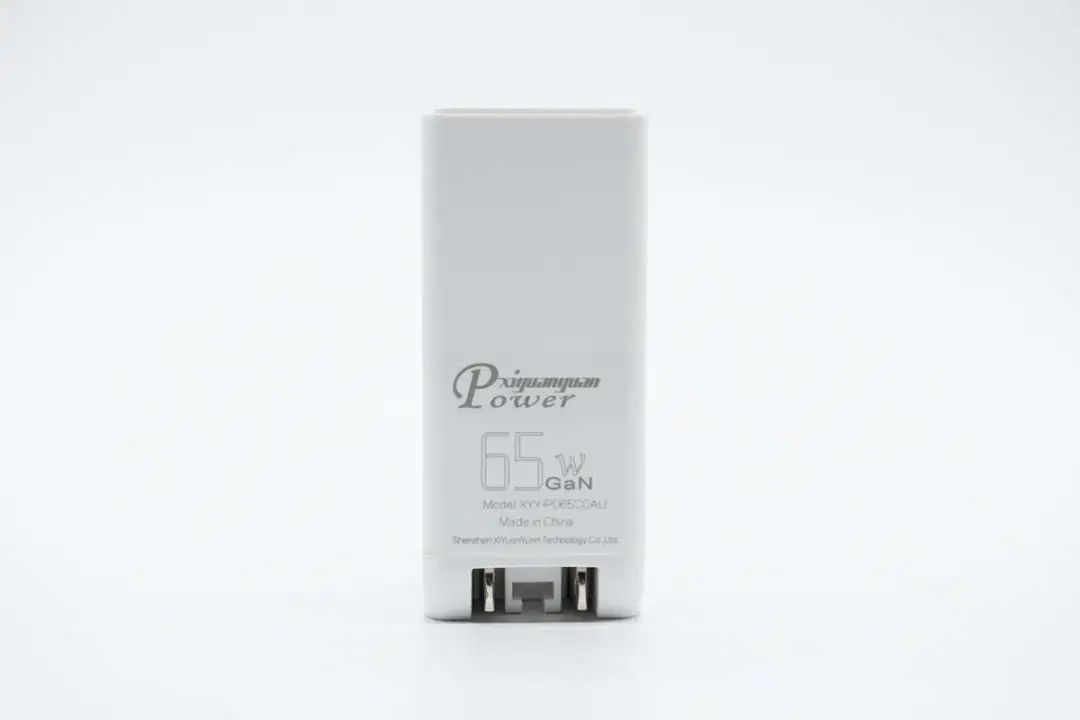
The waist side is printed with xiyuanyuan Power, 65W GaN, Model: XYY-PD65CCAU, and the full English name of Xiyuanyuan Company——ShenZhen XiYuanYuan Technology Co.,Ltd。

The product parameters are printed on the other side, and from the certification information, it can be seen that this gallium nitride charger is a product sold overseas.

Close-up of charger parameters
input:100-240V~50/60Hz 1.5A
Single port output:
USB-C1/C2:5V3A、9V3A、12V3A、15V3A、20V3.25A
USB-A:5V3A、9V3A、12V3A
Dual port output:
USB-C1+USB-C2:45W+20W
USB-C1+USB-A:40W+18W
USB-C2+USB-A:15W Max
Three port output:
USB-C1+USB-C2+USB-A:45W+15W
45W:5V3A、9V3A、12V3A、15V3A、20V2.25A
20W:5V3A、9V2.22A、12V1.67A
18W:5V3A、9V2A、12V1.5A
15W:5V1.5A+5V1.5A
The charger has passedUL、FCC、PSE认证。

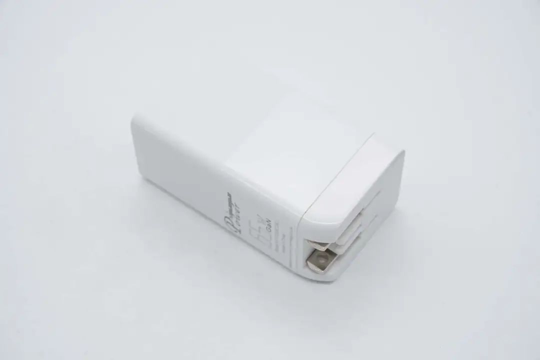
The charger is equipped with foldable American standard pins for easy portability.
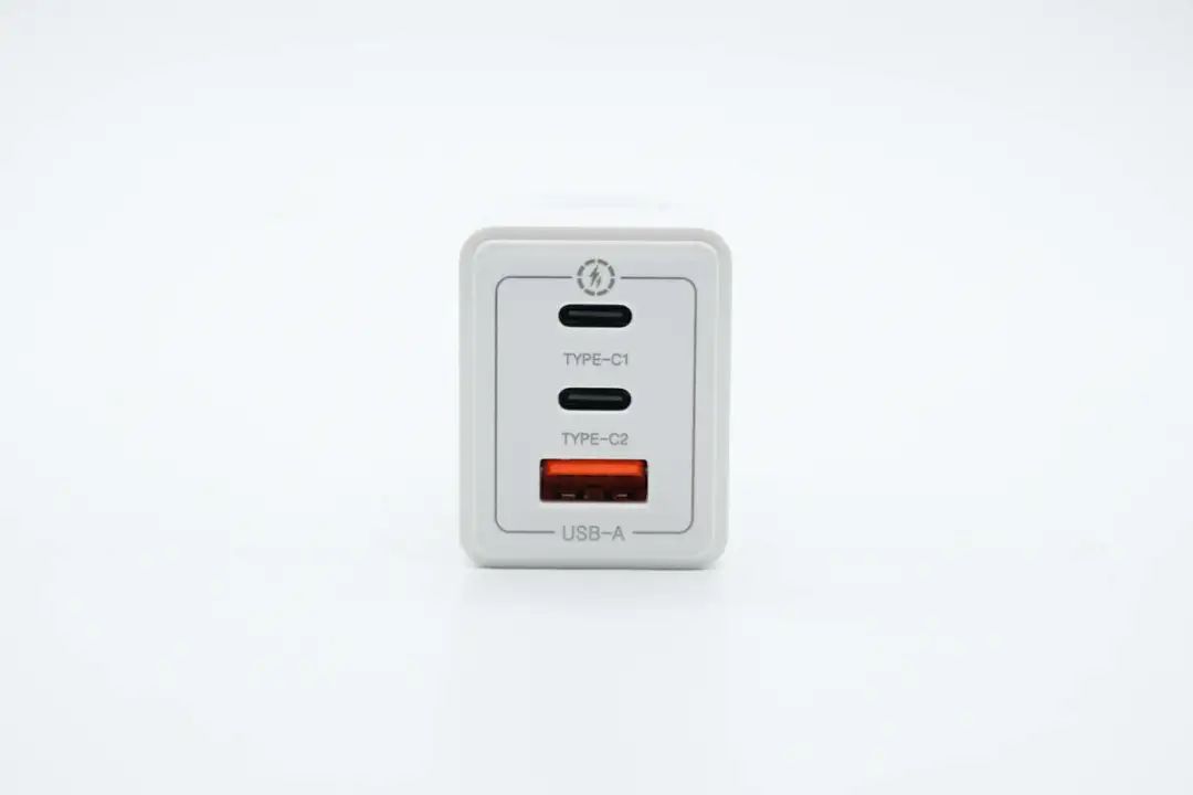
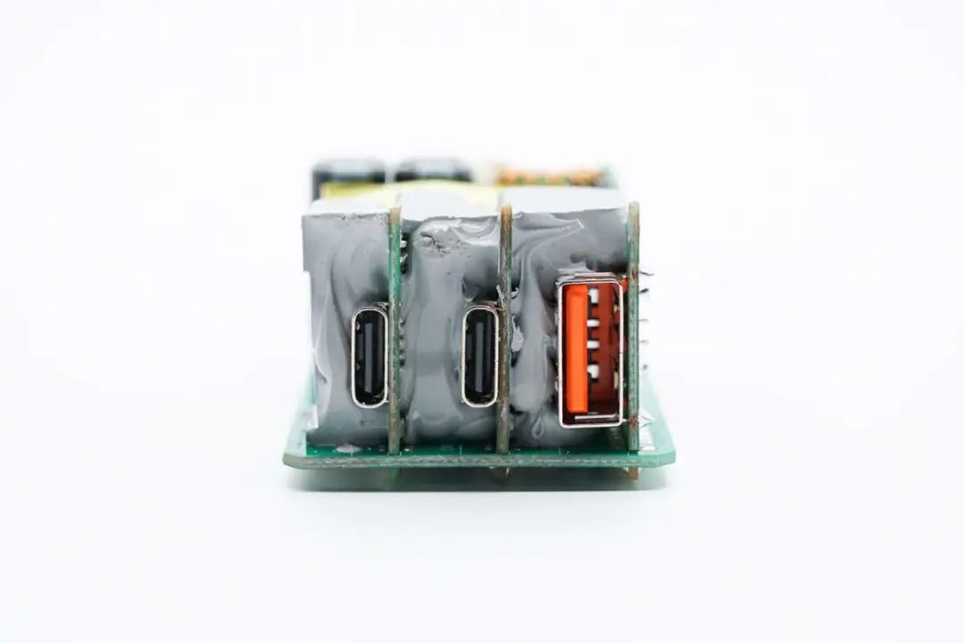
The output end is equipped with 2C1A three USB interfaces, with two types of interface rubber cores being black and orange red rubber cores.

The top edge of the fuselage is designed with a small circle, adding a sense of overall design.
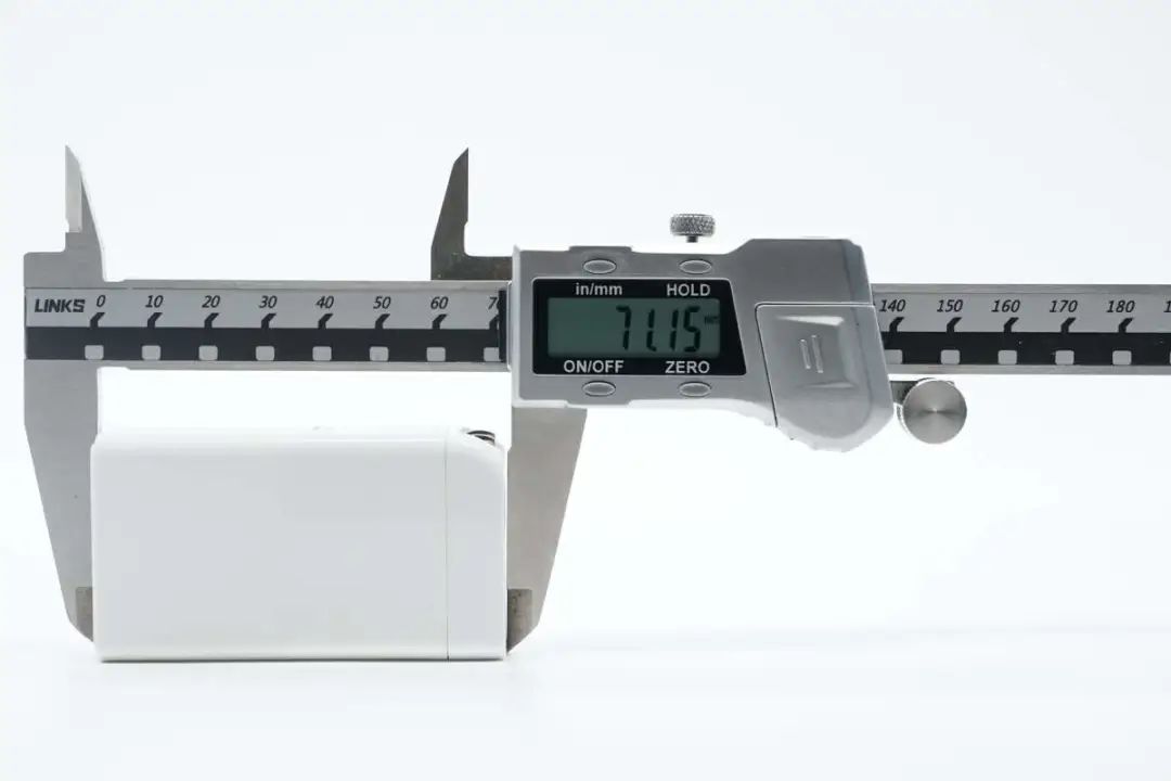
The measured length of the 65W GaN charger body of Xiyuan Source is 71.15mm.
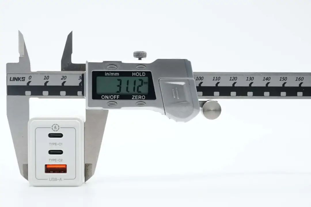
Width is31.12mm。
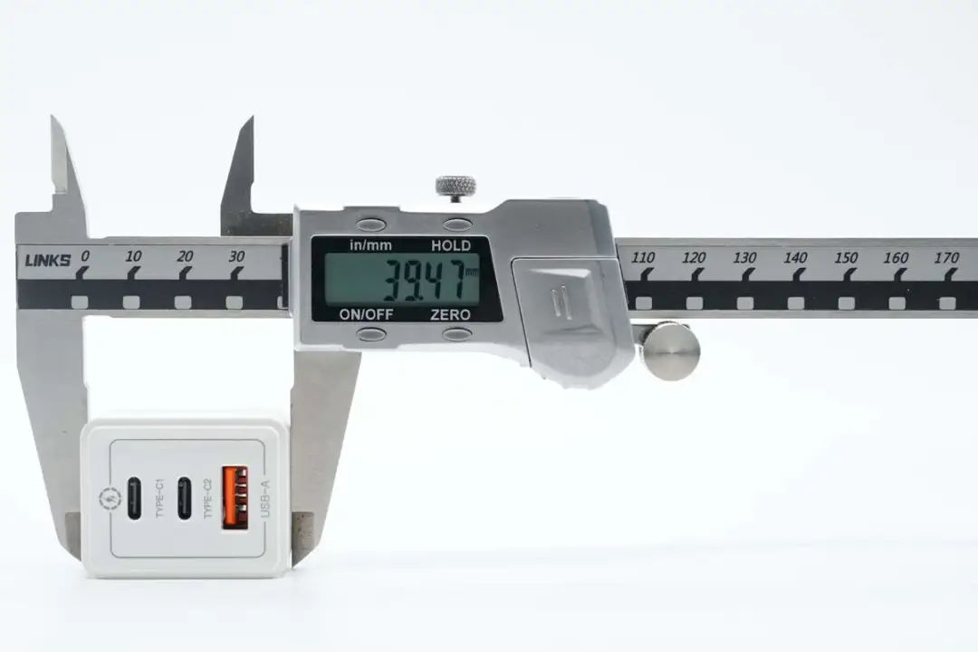
Thickness is39.47mm。
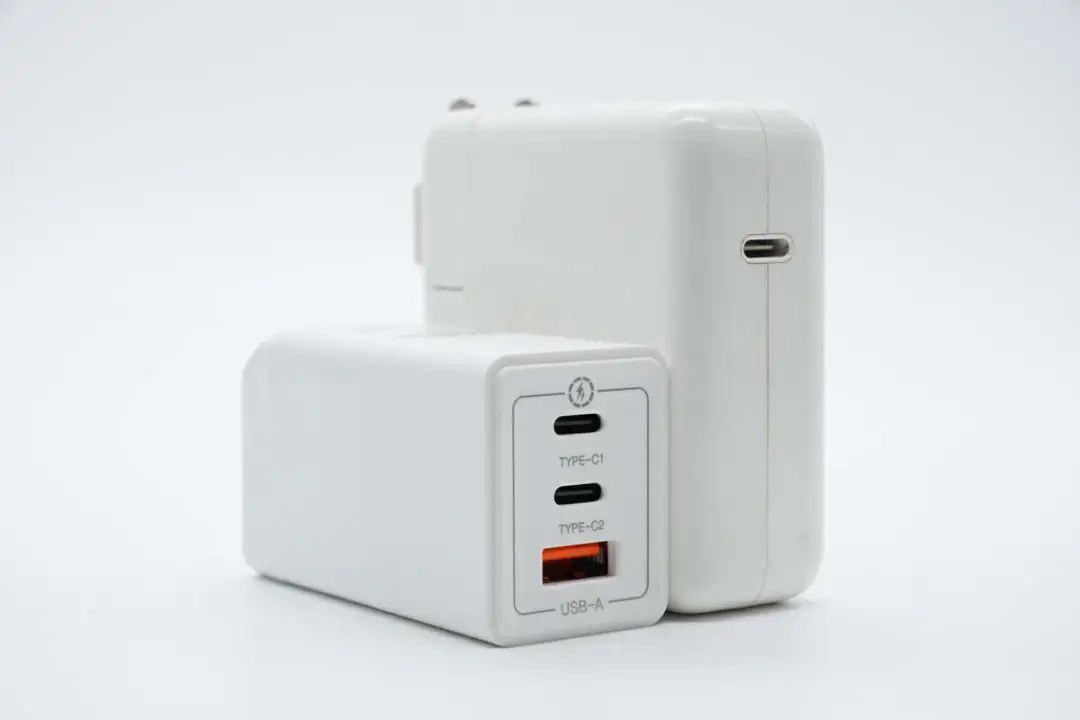
Compared to the Apple 61W charger, the size advantage is significant.

The size of the charger in hand is intuitive.
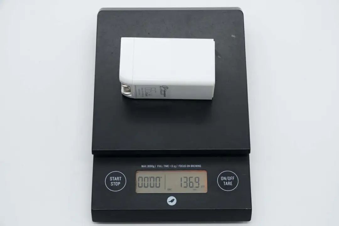
Additionally, the measured net weight of the charger is approximately137g。
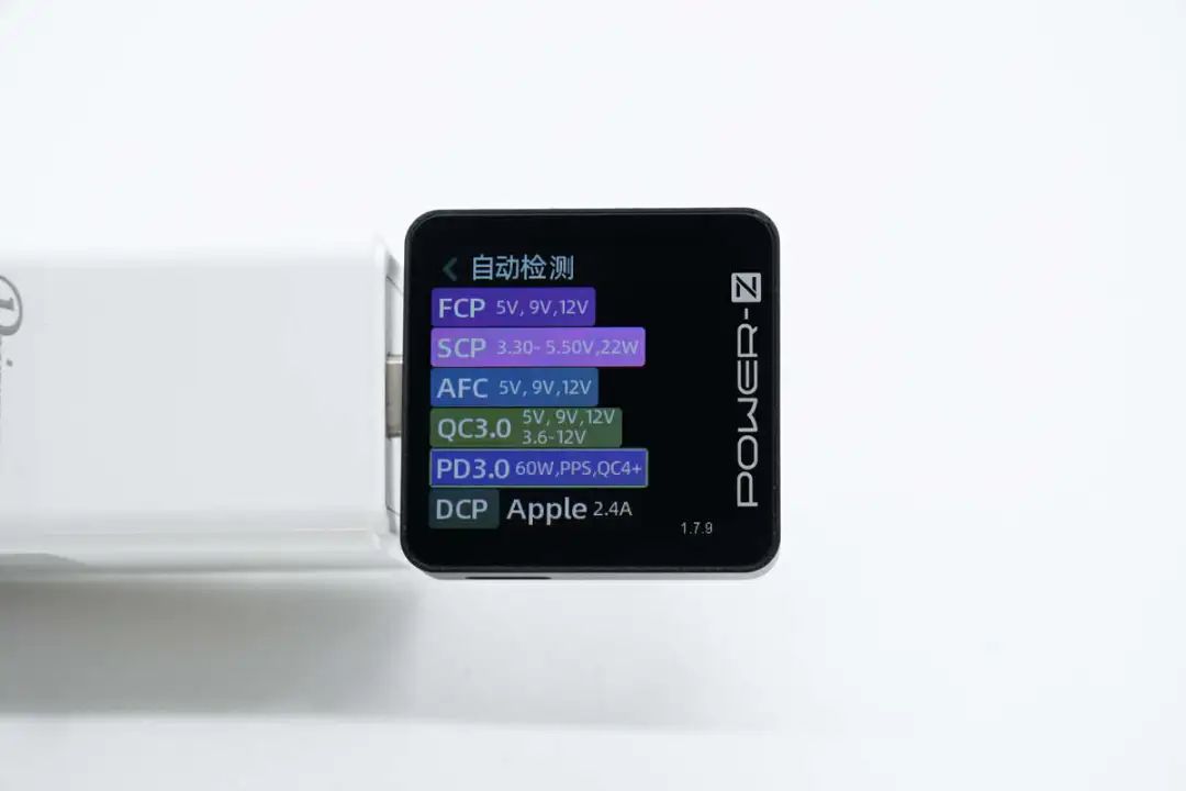
Using ChargerLAB POWER-Z KM003C, it was found that the USB-C1 port supports FCP, SCP, AFC, QC3.0/4+, PD3.0, PPS, DCP, and Apple 2.4A charging protocols.
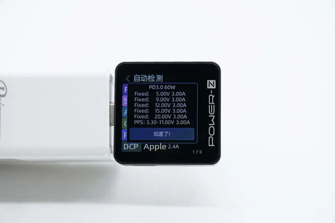
And it has five fixed voltage ranges of 5V3A, 9V3A, 12V3A, 15V3A, and 20V3A, as well as one PPS voltage range of 3.3-11V3A.
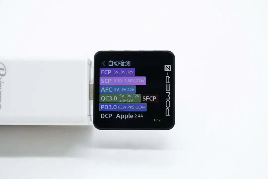
The USB-C2 port supports FCP, SCP, AFC, QC3.0/4+, SFCP, PD3.0, PPS, DCP, and Apple 2.4A charging protocols.
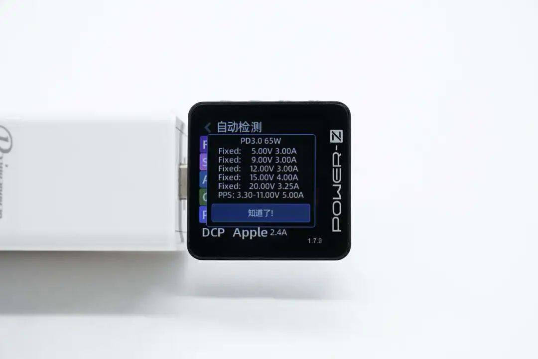
The PDO message shows that the USB-C2 port has five fixed voltage ranges of 5V3A, 9V3A, 12V3A, 15V4A, and 20V3.25A, as well as one PPS voltage range of 3.3-11V5A.
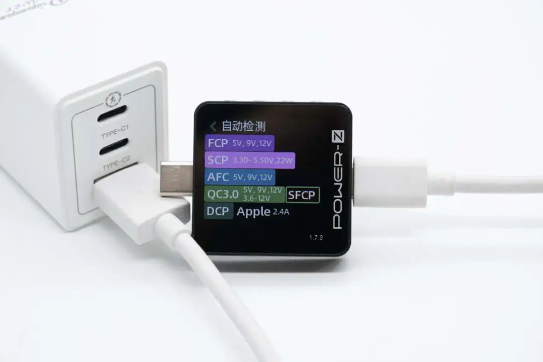
Finally, it was measured that the USB-A port supports FCP, SCP, AFC, QC3.0, SFCP, DCP, and Apple 2.4A charging protocols.
Disassembly of Xiyuanyuan 65W Gallium Nitride Charger
After reviewing the appearance and testing of this charger, we will now disassemble it and take a look at the internal design.
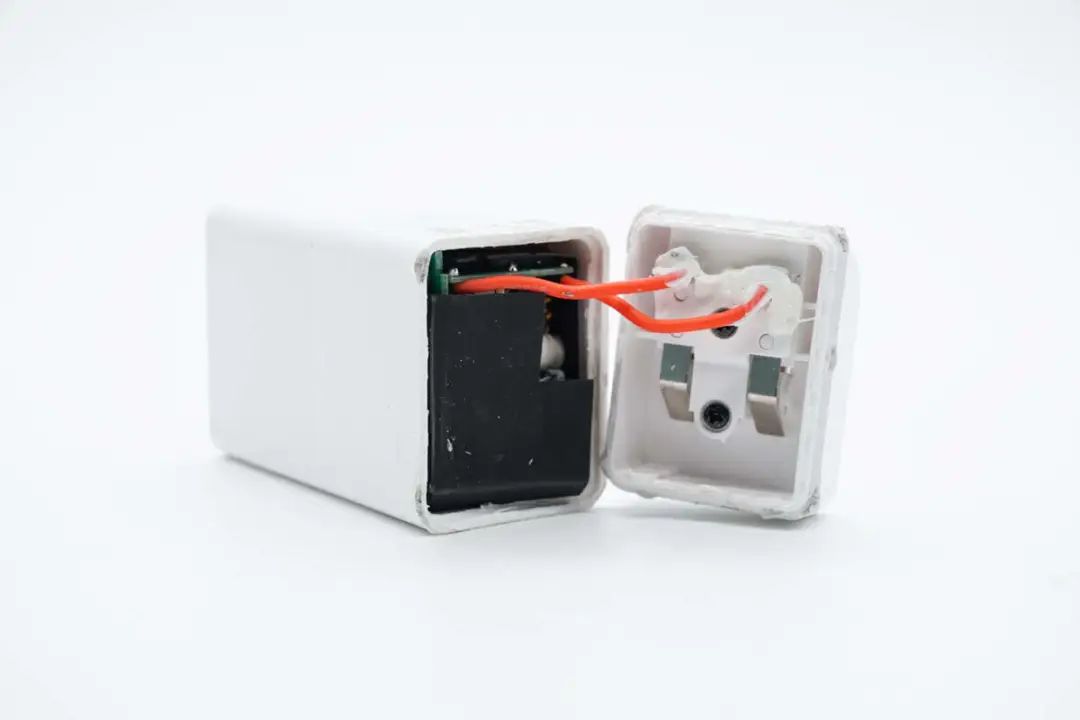
Firstly, disassemble the charger shell along the shell seam, fold the pins and connect them to the PCBA module through wire welding.

Apply adhesive to reinforce wire solder joints.

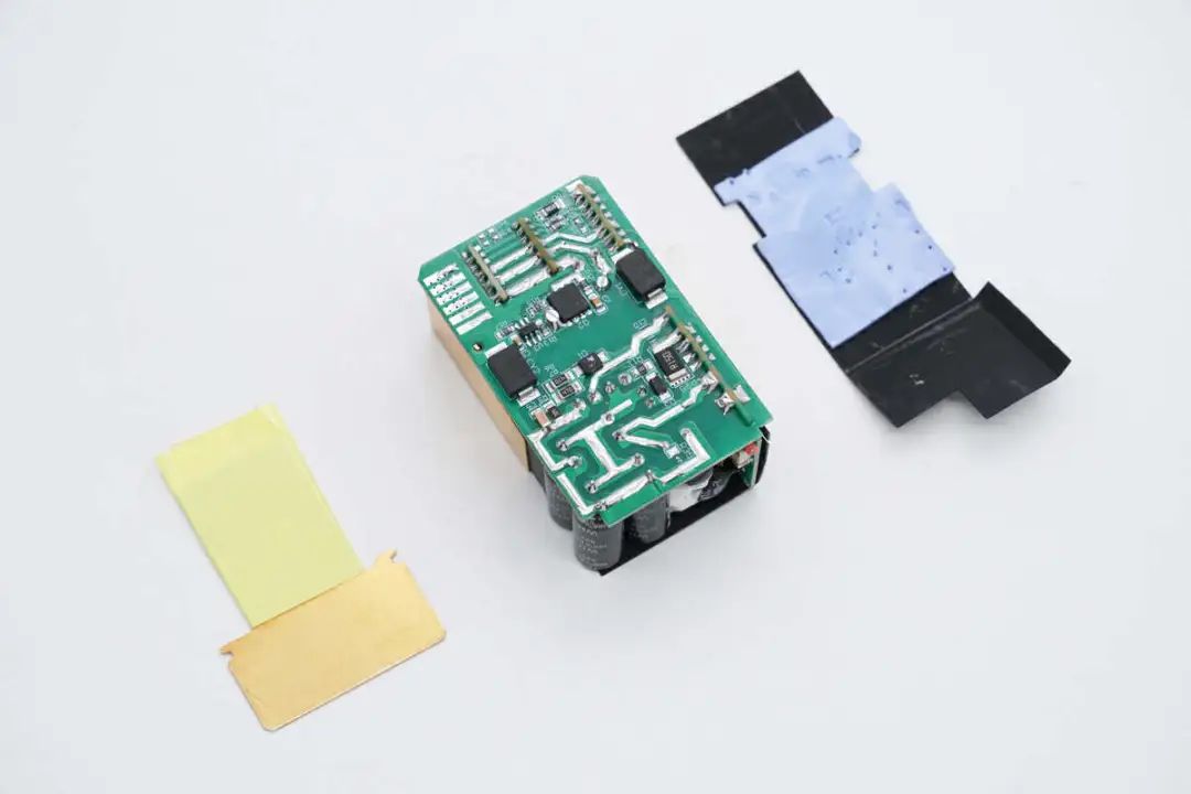
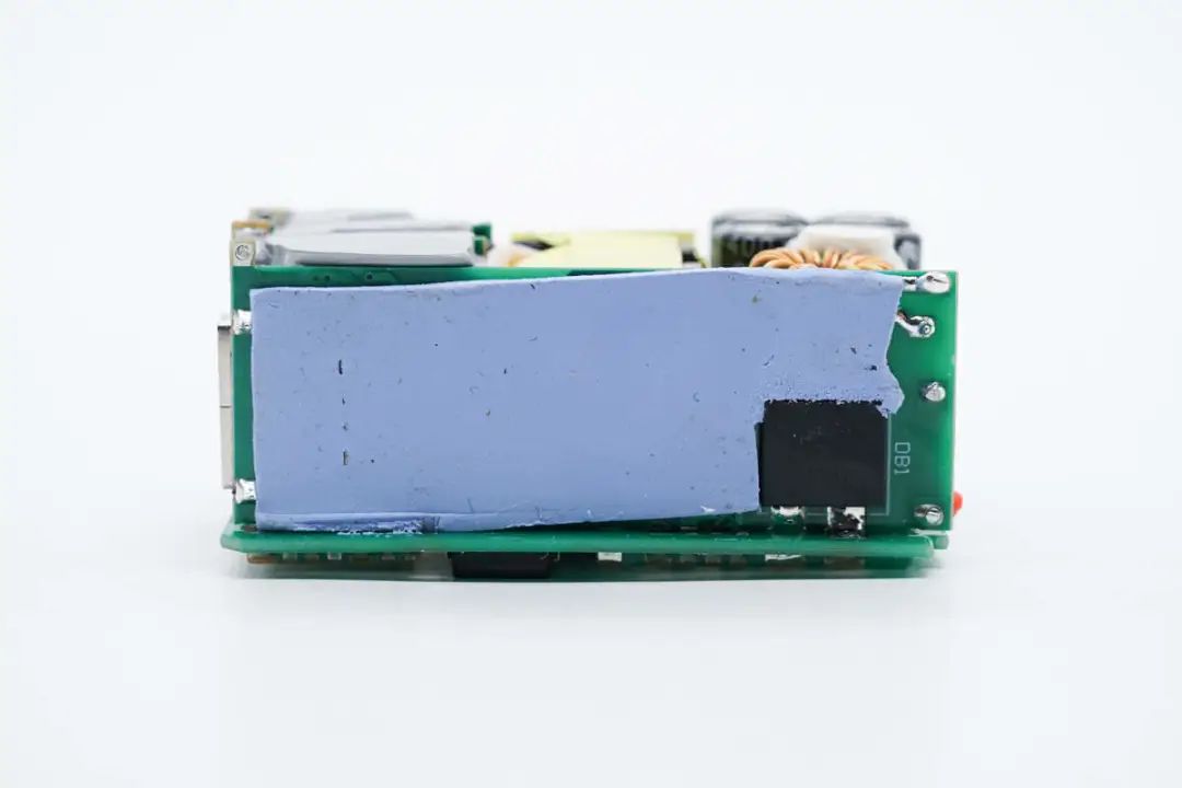
Extract the internal PCBA module, cover it with copper sheets for heat dissipation, and use Mylar sheet insulation.
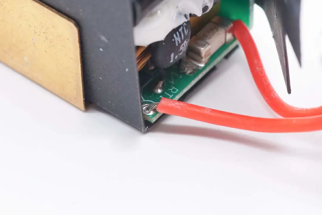
The wire is directly welded to the PCBA module for power supply.
The PCBA module is wrapped and insulated with Mylar sheets.
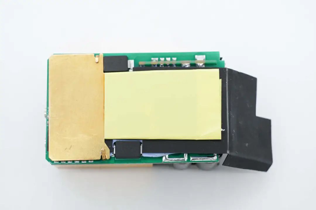
The copper strip on the back is wrapped with tape for insulation.
The back heat dissipation copper sheet is insulated with a Mylar sheet and a thermal conductive pad is pasted on the PCB.

The front heat sink is also insulated with Mylar sheets, and a thermal conductive pad is attached to the corresponding transformer position. The output voltage reducing circuit is coated with thermal conductive adhesive.
Thermal conductive pads are also pasted on the side of the PCBA module to help dissipate heat.

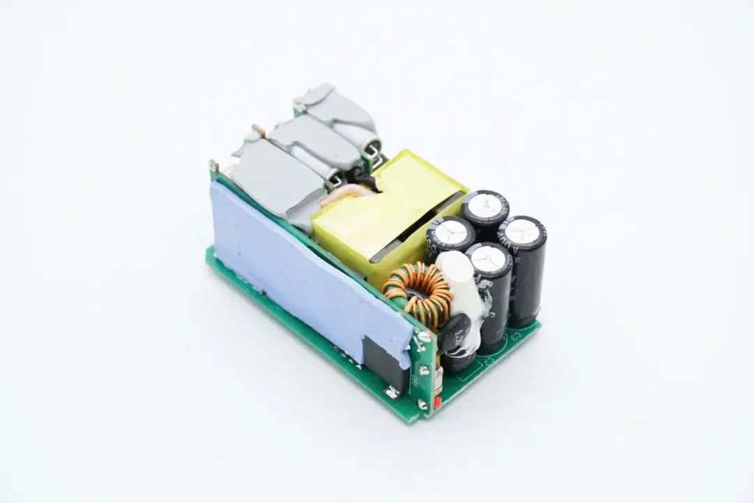
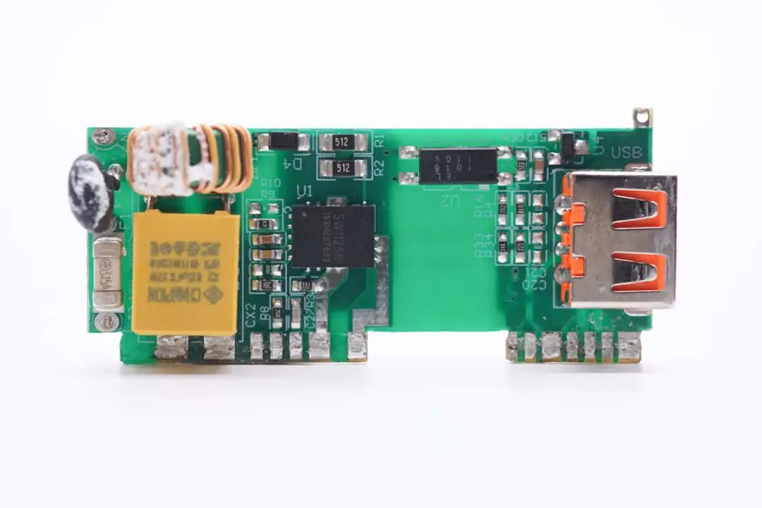
At the front of the PCBA module, there is an output secondary step-down circuit on the left, a transformer in the middle, and an input EMI circuit and high-voltage filtering capacitor on the right. A small board is welded on the side to connect the primary stage.
The back of the PCBA module is welded with a synchronous rectifier controller and synchronous rectifier tube, and two SMD Y capacitors are welded up and down.
Stick thermal conductive pads on the side panels to dissipate heat.
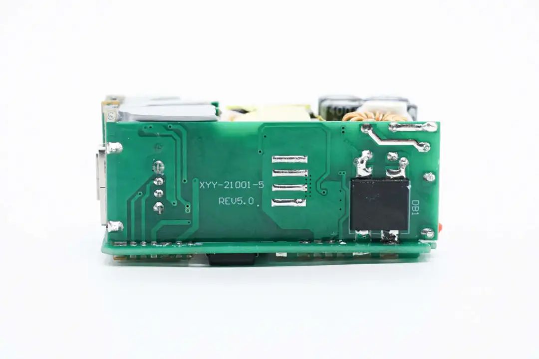
Weld a rectifier bridge on the side of the small board.
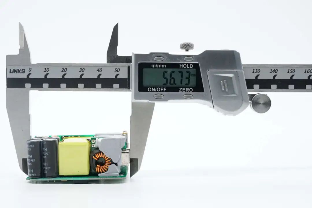
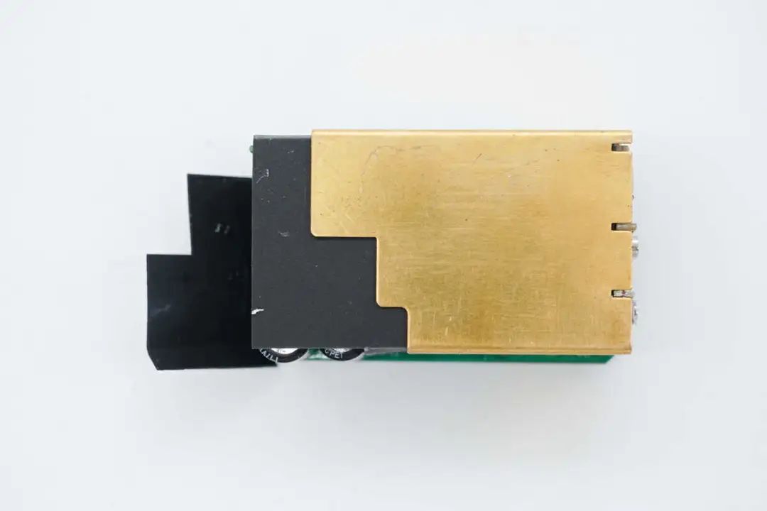
The length of the PCBA module measured using a vernier caliper is approximately56.7mm。
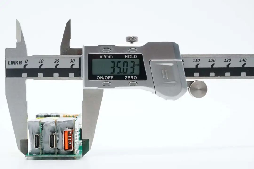
The width of the PCBA module is approximately 35mm.
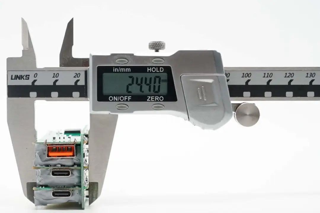
The thickness of the PCBA module is approximately 24.4mm.
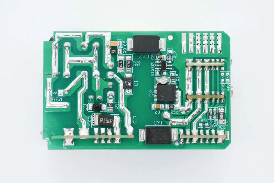
Welding fuses on the front of the side panel, NTC thermistors, common mode inductors, and safety regulated X2 capacitors. Gallium nitride sealing chip, feedback optocoupler, and USB-A interface.
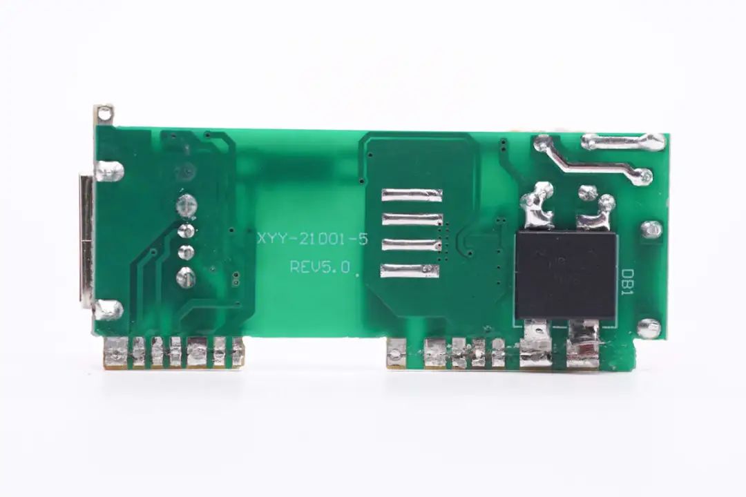
A rectifier bridge is welded on the back of the side panel, corresponding to the exposed copper and tin heat dissipation on the back of the gallium nitride sealed chip.
Through observation of the PCBA module, it was found that this 65W gallium nitride charger adopts a flyback switching power supply design, paired with synchronous rectification, and has a fixed voltage output. The output adopts two independent synchronous step-down circuits, achieving three port fast charging output and automatic power distribution function. Let's start from the input end to understand the design and materials of the entire charger.

The specification of the input delay fuse is 3.15A, with patch welding.
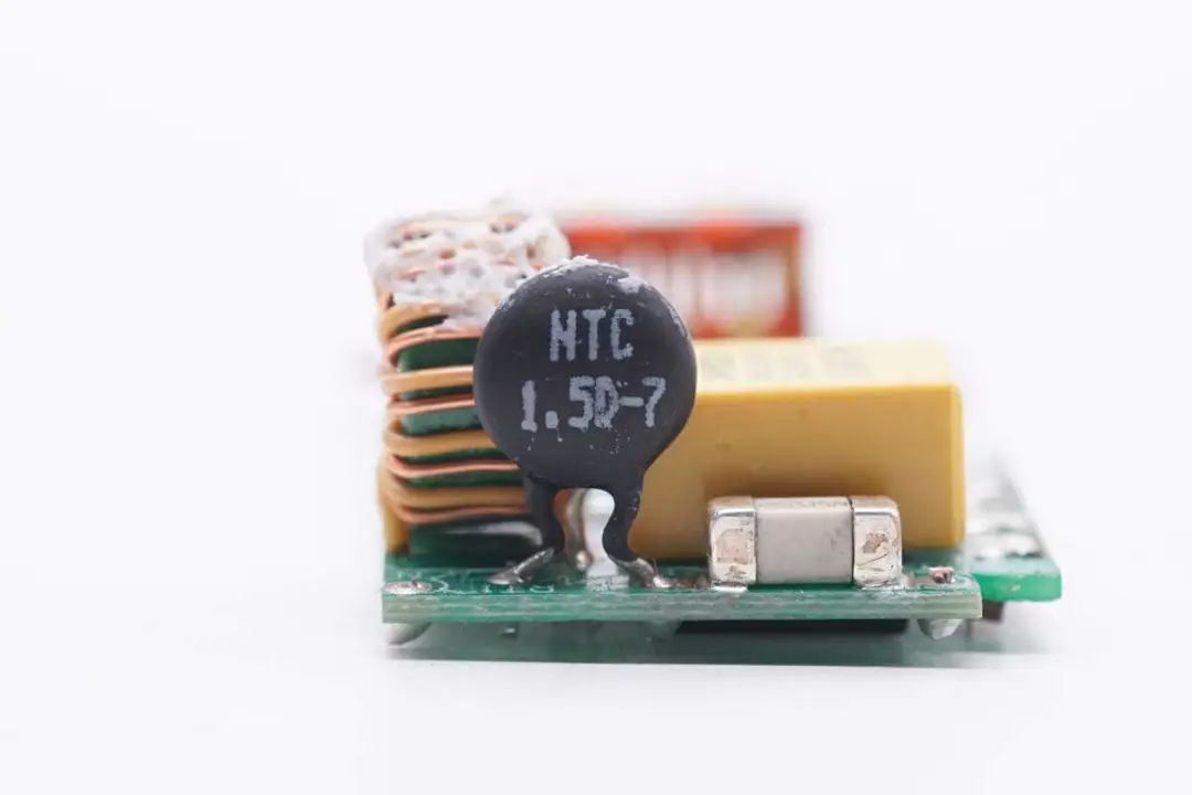
NTC thermistor screen printing 1.5D-7.
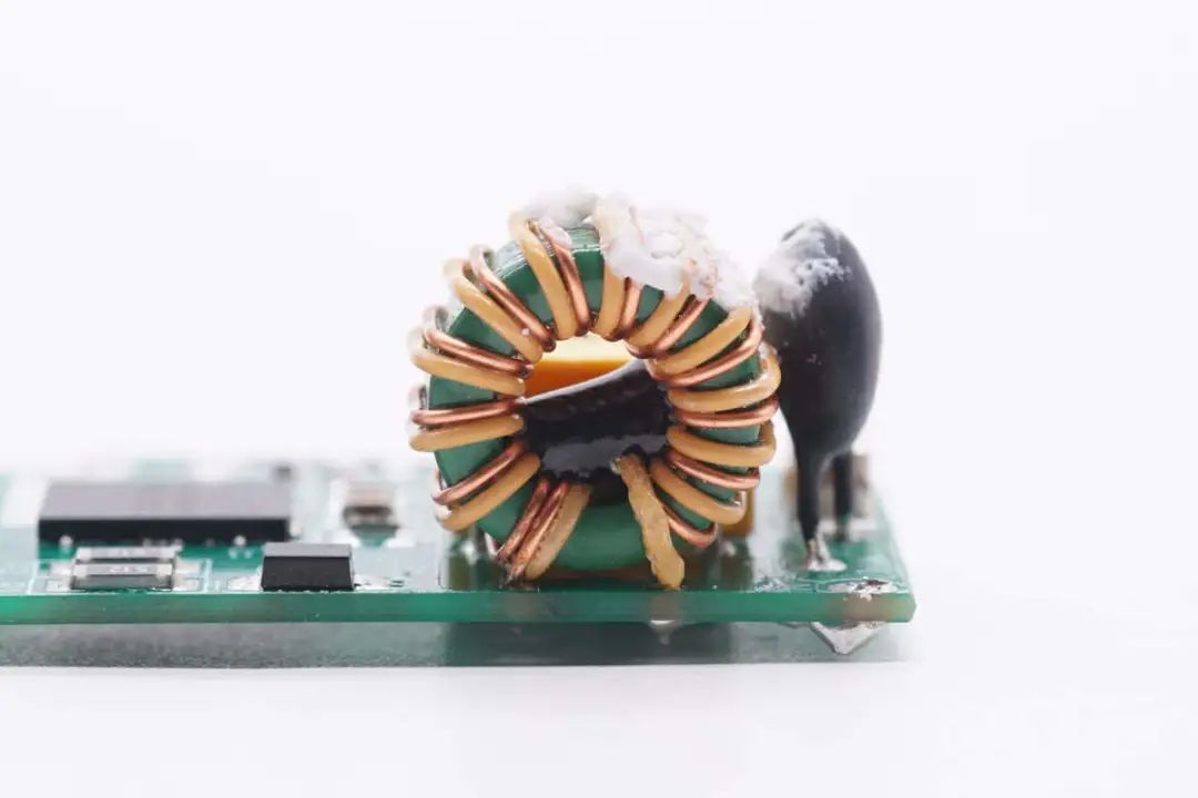
The common mode inductor is wound with enameled wire and insulated wire.
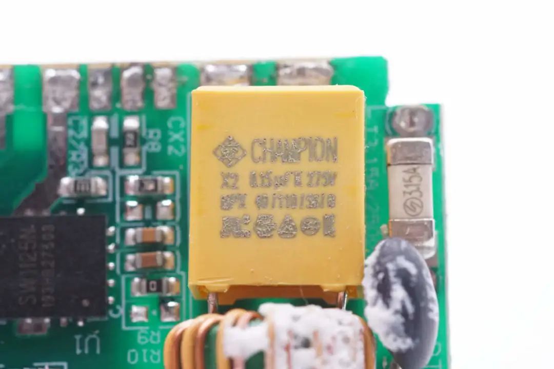
The safety regulation X2 capacitor comes from CHAMPION Quanpeng Electronics, with a specification of 0.15 μ F.

A rectifier bridge is welded on the back of the small board, from Shenzhen Wald Industrial Co., Ltd., model WRLSB80M. This soft bridge has a relatively soft recovery curve and smooth turn-off characteristics, which can reduce the diode junction capacitance and achieve very little harmonic oscillation. The selected LSB packaging has good heat dissipation characteristics, helping to improve the reliability of medium to large wattage adapters. A single adapter can be used for 60W+.
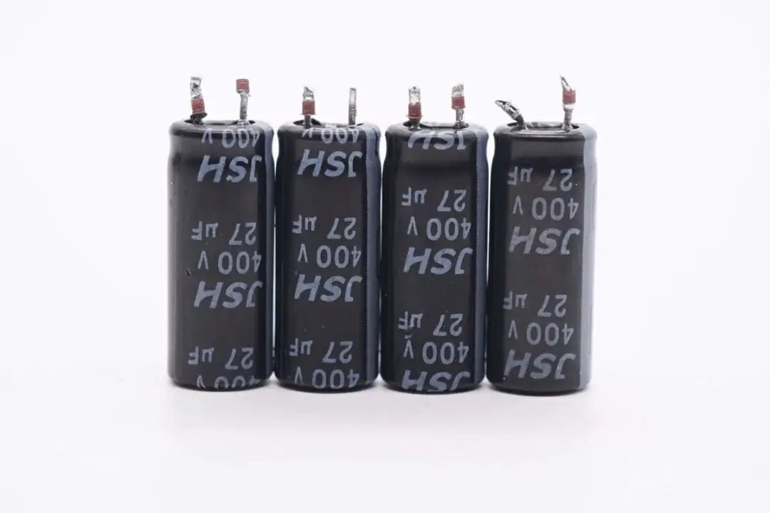
The high-voltage filtering capacitor comes from JSH Wanjingyuan, with a specification of 400V 27 μ F.

The differential mode inductor is wound with a magnetic ring and insulated with a heat shrink tube.
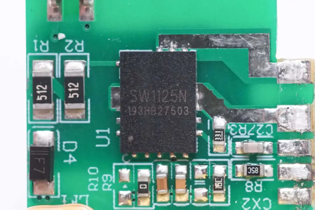
The charger is equipped with a built-in Zhirong SW1125 sealed gallium nitride chip, which is a high-frequency quasi resonant flyback converter that integrates a 650V withstand voltage and 260m Ω resistive gallium nitride switch transistor. The chip integrates a 700V high-voltage startup circuit, line voltage power-off detection, and X capacitor discharge function.
SW1125 operates in the valley bottom open mode with valley bottom locking, reducing switch losses, and integrating frequency jitter function to optimize EMI performance. The chip supports burst mode and automatically enters burst mode to optimize light load efficiency when the load decreases. The idle power consumption is less than 50mW, meeting the six level energy consumption requirements.
SW1125 supports a wide range of power supply of 7-90V, supports a maximum switching frequency of 300KHz, and adopts a QFN6 * 8 package with enhanced heat dissipation. It can reduce chip temperature rise through through-hole heat conduction, optimize wiring, and simplify heat dissipation design. The chip is equipped with multiple comprehensive protection functions and supports external NTC detection of charger temperature rise, achieving comprehensive protection design.
Detailed information of Zhirong SW1125.
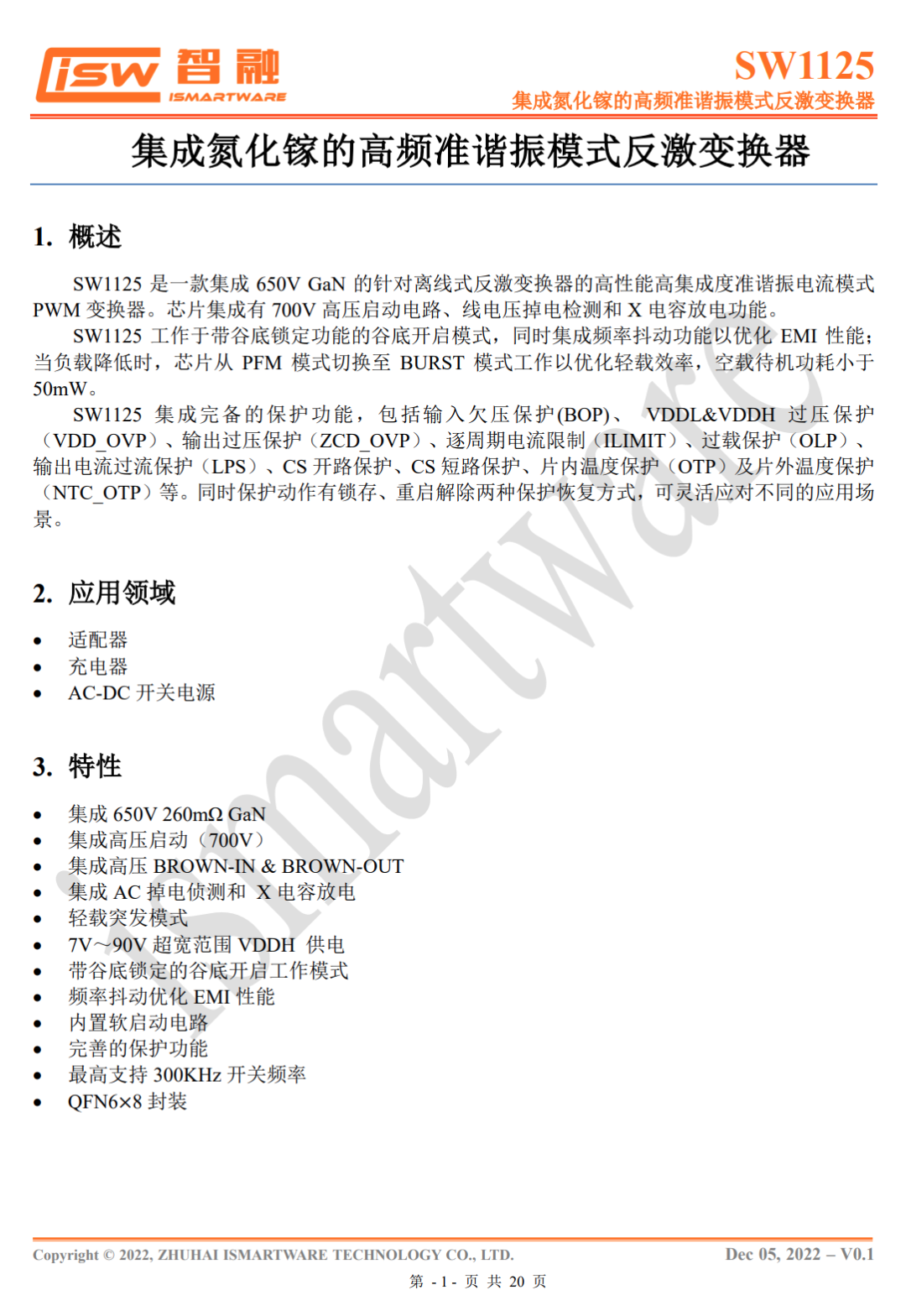
A 150m Ω sampling resistor is used to detect primary current.
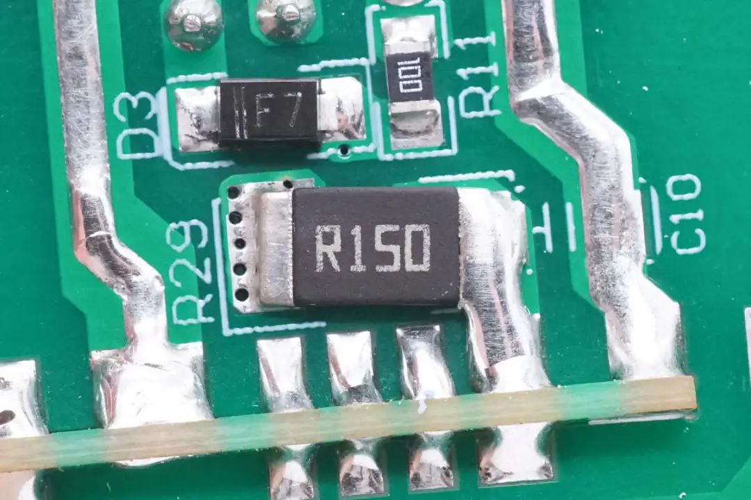
ten μ The F 50V electrolytic capacitor is used to power gallium nitride sealed chips.
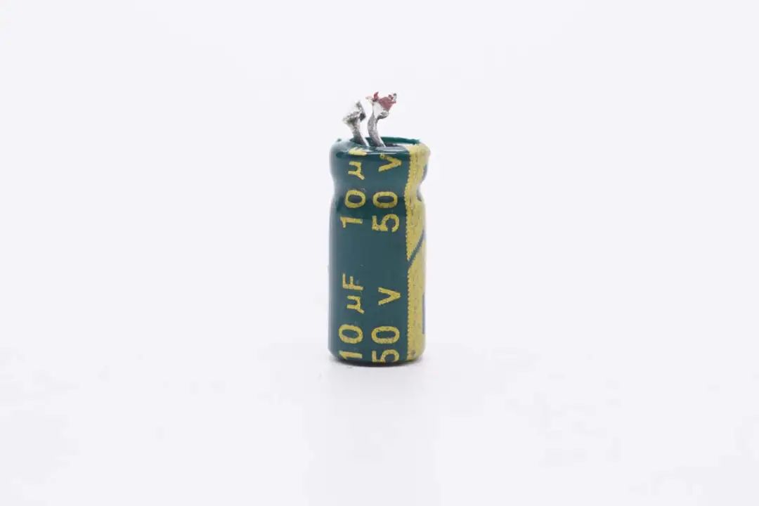
The transformer is labeled XYY-PD65W, indicating that it comes from Xiyuan Source and has a specification of 65W.
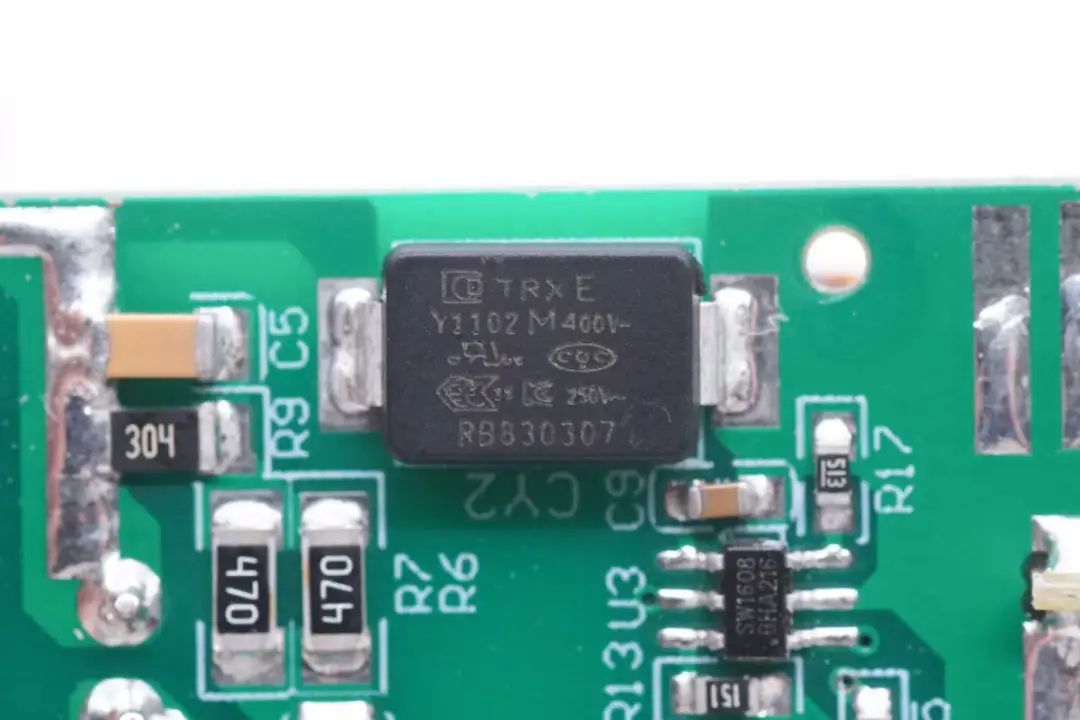
The SMD Y capacitor comes from Sichuan Teruxiang Technology Co., Ltd. It has characteristics such as small size and light weight, and is very suitable for use in high-density power products such as gallium nitride fast charging. The part number is TMY1102M.
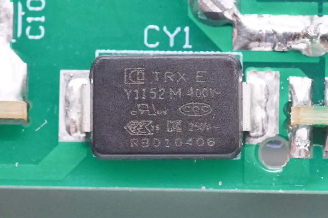
The material number of the other SMD Y capacitor is TMY1152M.

Yiguang EL1018 optocoupler is used for output voltage feedback.
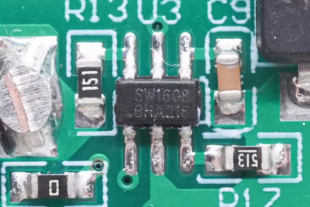
The synchronous rectification controller adopts Zhirong SW1608, which is a high-performance controller driven by the secondary synchronous rectification transistor (MOSFET) for offline flyback converters. It is packaged in SOT23-6 and supports 6V or 9V VCC power supply. The VCC has self power supply function, does not require auxiliary winding power supply, and supports a wide output voltage range. In combination with MOSFET, using alternative Schottky rectification diodes can significantly improve system efficiency.

SW1608 supports a working frequency of 600KHz and multiple application scenarios of High Side/Low Side, as well as multiple working modes of CCM/QR/DCM. In addition, its internal integrated intelligent conduction detection function can effectively prevent misleading conduction caused by DCM ringing; The chip also has ultra-low shutdown transmission delay time and strong pull-down current capability, which can significantly reduce the voltage stress of the rectifier tube.
According to the disassembly of the charging head network, the SW1125/SW1106+SW1608 gallium nitride power supply solution of Zhirong Technology was previously adopted by products such as Xiwei 100W 3C1A ultra high cost performance gallium nitride fast charging, Juhai 65W 2C1A gallium nitride charger, and Hongda Shun 65W three USB-C port gallium nitride charger.
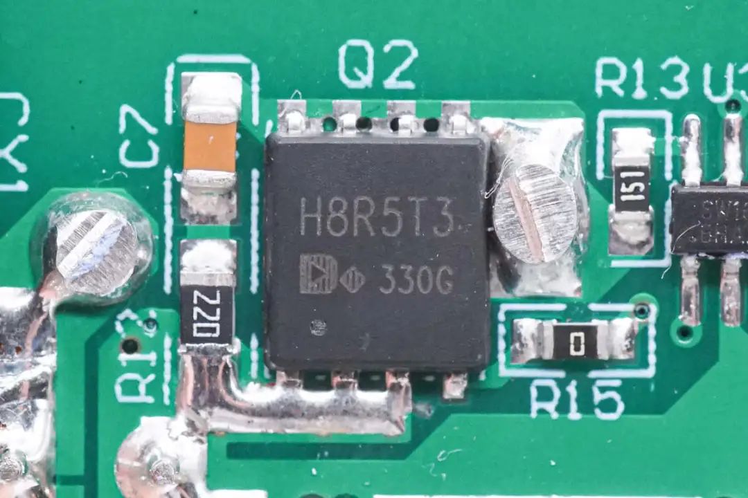
Synchronous rectifier tube screen printing H8R5T3.
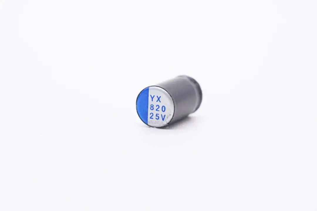
The output filter capacitor comes from YX Cloud Star, with a specification of 820 μ F 25V.
The output terminals USB-C and USB-A are respectively welded to independent small boards, and the voltage reducing circuit is coated with glue for heat dissipation.
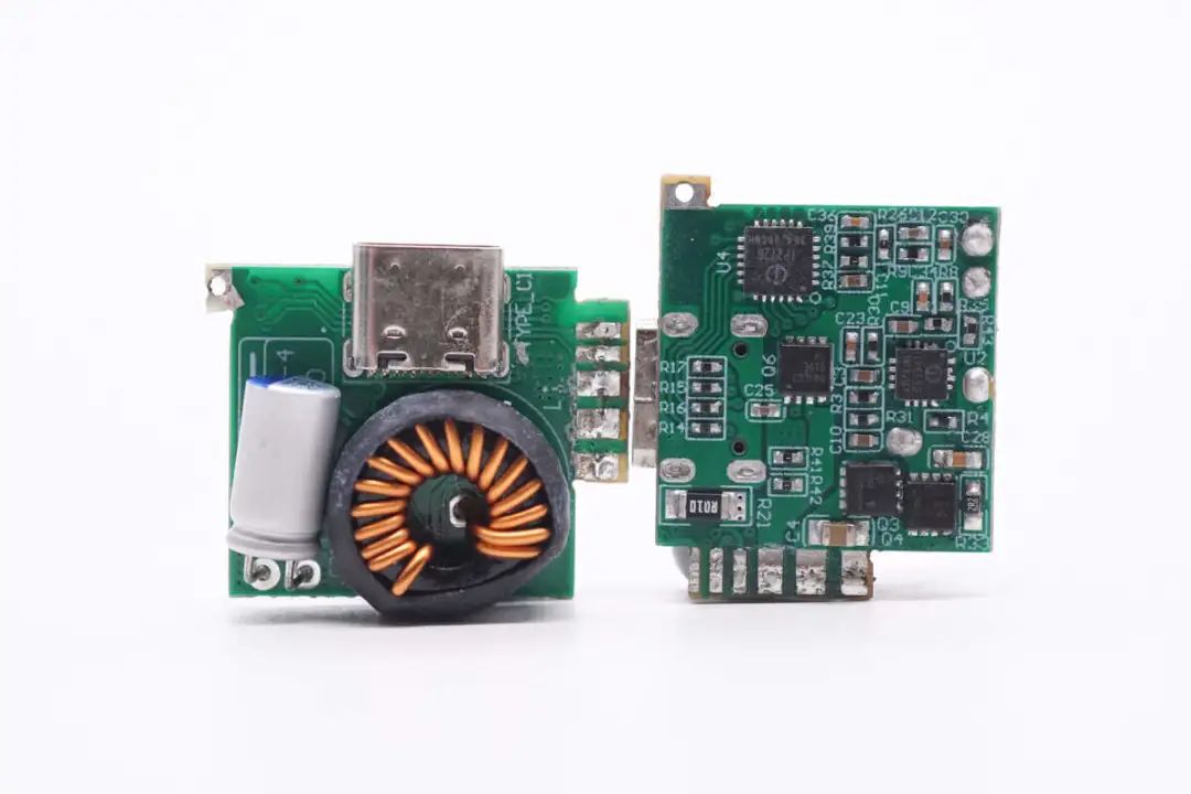
Close up of the front and back sides of the two voltage reduction boards, with one side welded with a voltage reduction inductor, filter capacitor, and USB-C base, and the other side welded with a protocol chip, synchronous voltage reduction controller, voltage reduction switch tube, and VBUS switch tube.

The USB-C protocol chip adopts the IP2723T of the Intel chip, which has been certified by the USB IF Association PD3.0 PPS with TID: 3135. It is a fast charging protocol IC that integrates multiple protocols and is used for USB output ports. Supports multiple fast charging protocols, including USB TypeC DFP, PD2.0/3.0, PPS, HVDCP QC4, QC4+, QC3.0/2.0, FCP, SCP, AFC, MTK PE+2.0/1.1, Apple 2.4A, BC1.2, and Samsung 2.0A. On the right is the TVS protection tube of the USB-C base, used for electrostatic protection function.
We can provide a complete TYPE-C solution for one-way output applications such as adapters and car chargers. In addition, IP2723T has high integration and rich functionality, requiring only a few peripheral devices during application, effectively reducing the overall size of the solution and reducing BOM costs.
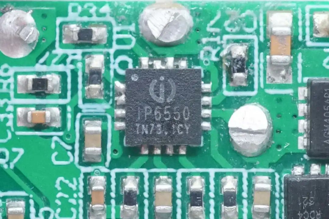
The synchronous rectification and voltage reduction controller used for voltage reduction output is from Yingjixin, model IP6550. It is a synchronous voltage reduction controller that supports 36V input, with built-in NMOS transistor driver and two external MOS transistors for efficient synchronous rectification and voltage reduction. IP6550 adjusts the output voltage through the feedback pin. Switching frequency 135KHz, input terminal withstand voltage 48V, built-in complete protection function. The Yingjixin IP6550 adopts a 3 * 3mm QFN16 packaging, which can achieve a simplified synchronous buck conversion circuit design.
IP6550 can be used for car chargers, multi port adapters, intelligent plugins, plugins that support USB-C interfaces, and dash cam applications. Synchronous rectification and voltage reduction have high conversion efficiency, and the high output current can be used for multi port 5V output. With the PD protocol chip, it can achieve wide range voltage regulation, meeting the application of USB PD3.1.
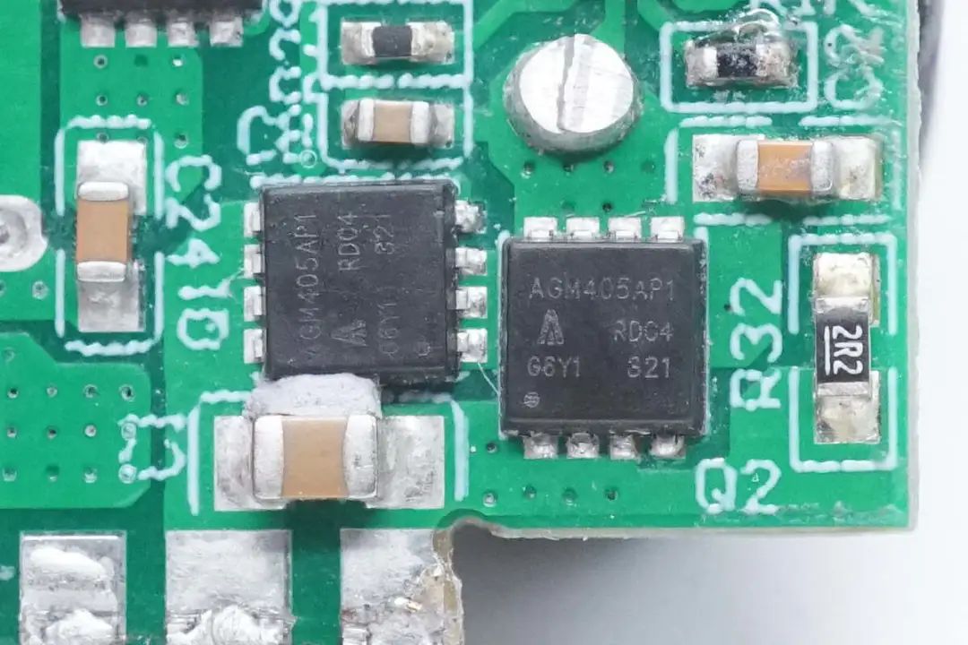
Two step-down switch tubes come from the core control source, model AGM405AP1, which is a 40V withstand NMOS with a conductivity of 5.7m Ω and is packaged in DFN3.3 * 3.3.
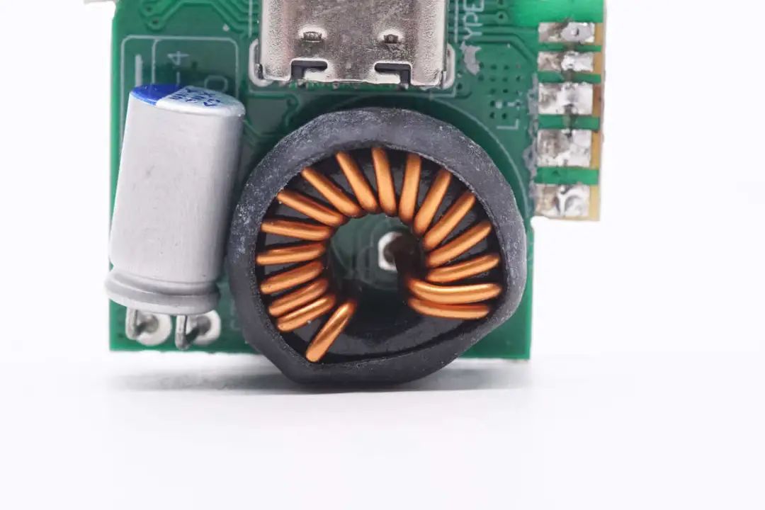
The step-down inductor is wound with a magnetic ring and insulated with a heat shrink tube.

The output filter capacitor comes from YX Cloud Star, with a specification of 220 μ F 25V.
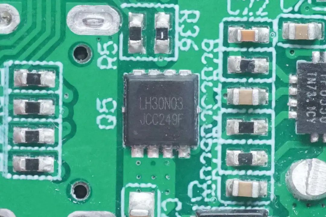
The VBUS switch tube used for the USB-C1 interface is from Li Macro Micro, model LH30N03. It is a 30V withstand NMOS with a conductivity of 9m Ω and is packaged in DFN3 * 3.

A 10m Ω resistor is used for output current detection.

The VBUS switch tube used for USB-C2 and USB-A ports is from Guanyu, model KS3418MB. It is a 30V withstand dual N MOS with a conductivity of 7m Ω and is packaged in PDFN3333.
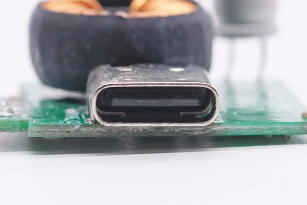
The USB-C interface is fixed by via welding, and the black rubber core does not expose copper.
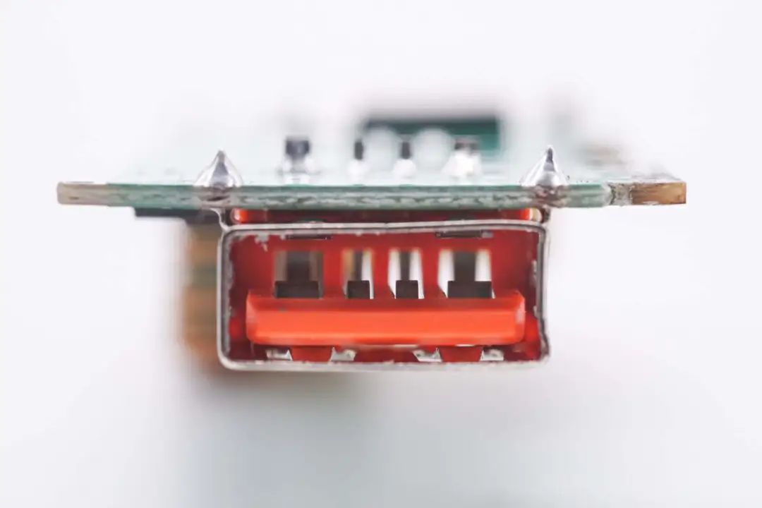
The USB-A interface adopts an orange rubber core, and the positive and negative poles are widened to support high current fast charging.
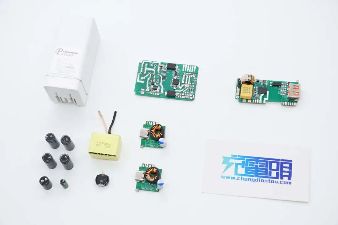
Complete disassembly and a family photo.
Summary of dismantling the charging head network
Xiyuan Yuan's gallium nitride charger is designed with foldable pins, making it compact and easy to carry in daily life. The charger has a 2C1A output interface, and the USB-C port supports dual port blind insertion and automatic power allocation, which can charge both mobile phones and computers simultaneously. In addition, it also supports PPS fast charging, which has good compatibility with new and old devices for fast charging.
According to the disassembly of the charging head network, this charger is equipped with a smart integrated technology SW1125 sealed gallium nitride chip. This chip integrates a gallium nitride switch transistor and high-frequency flyback driver, as well as a high-voltage starting circuit and X capacitor discharge function. The chip supports a wide range power supply of 7-90V, which is applied in PD fast charging without the need for additional power supply windings or voltage stabilizing circuits, further simplifying the application.
At the same time, an internal intelligent integration SW1608 synchronous rectifier controller is also used, which is combined with synchronous rectifier tubes to form a fixed voltage output switching power supply. The output adopts two British chip IP2723T protocol chips paired with an IP6550 synchronous step-down controller. The PCBA module adopts copper sheets to enhance heat dissipation, and corresponding heating devices are pasted with thermal conductive pads to accelerate heat conduction and reduce the temperature rise of high-power fast charging.
